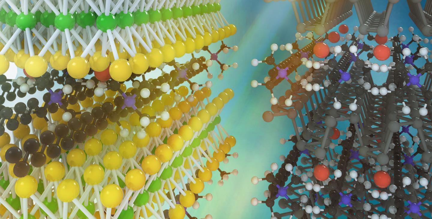
A research team comprised of UCLA scientists and engineers has managed to develop two-dimensional materials that are only one or two atoms thick which behave differently to other state-of-the-art superlattices.
Superlattices are two-dimensional materials made up of alternating layers of ultra-thin sheets. While the development of a superlattice has already been accomplished, the UCLA team has managed to develop two-dimensional materials that can have radically different structures, properties, and functions – a process that was not previously available.
These new two dimensional materials have the potential for application in many areas due to their abilities to enhance electronics. One such application may be two different layers: one to allow a quick flow of electrons, and the other to act as an insulator. The two-dimensional materials act independently and are their own layers, and this separation prevents them from interfering with other materials. The researchers believe these new materials show great potential for inclusion in “superfast and ultra-efficient semiconductors for transistors in computers and smart devices, and advanced LEDs and lasers.”
In addition to having the capability to separate different functions, the manufacturing process of these new two dimensional materials is much faster and more efficient. And while traditional superlattices only have a few layers, this new process can produce material with thousands of alternating layers – an achievement that hasn’t been possible until now.
The study describing these new materials was published in Nature, and led by Xiangfeng Duan, UCLA professor of chemistry and biochemistry, alongside Yu Huang, UCLA professor of materials science and engineering at the UCLA Samueli School of Engineering.
“Traditional semiconductor superlattices can usually only be made from materials with highly similar lattice symmetry, normally with rather similar electronic structures,” Huang said. “For the first time, we have created stable superlattice structures with radically different layers, yet nearly perfect atomic-molecular arrangements within each layer. This new class of superlattice structures has tailorable electronic properties for potential technological applications and further scientific studies.”
Current methods to build two-dimensional materials are to either stack the ultrathin layers on top of each other, or to grow a new layer on top of another using “chemical vapor deposition”. Both of these methods are labor intensive, require specialized equipment, and are not reliable – often ending up with an altered or broken bottom layer. This new method uses a new process called “electrochemical intercalation” where the scientists applied a negative voltage. This voltage puts negatively charged electrons into the two-dimensional materials which attracts positive ammonium molecules – automatically assembling them into new layers and creating a superlattice.
“Think of a two-dimensional material as a stack of playing cards,” Duan said. “Then imagine that we can cause a large pile of nearby plastic beads to insert themselves, in perfect order, sandwiching between each card. That’s the analogous idea, but with a crystal of 2D material and ammonium molecules.”
“The resulting materials could be useful for making faster transistors that consume less power, or for creating efficient light-emitting devices”


